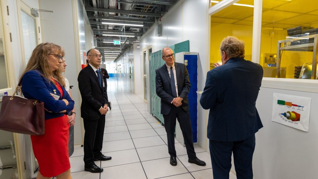
A cutting-edge facility employing pioneering e-beam technology to develop the next generation of semiconductor chips was officially opened at the University of Southampton by science minister Lord Patrick Vallance.
This new e-beam lithography facility is only the second of its kind globally, and the first to be located outside of Japan. It offers exceptional accuracy, which is crucial for designing the minute components that power future technologies, ranging from medical diagnostics to defence systems.
Semiconductors, the small chips that power devices from smartphones to satellites, already contribute an estimated £10 billion annually to the UK economy, with the sector projected to grow to approximately £17 billion by 2030. Lord Vallance inaugurated the new facility alongside Southampton’s vice-chancellor Professor Mark E Smith and Professor Graham Reed, who leads the university’s Optoelectronics Research Centre (ORC) and prototyping foundry CORNERSTONE.
Lord Vallance said: “Britain is home to some of the most exciting semiconductor research anywhere in the world. Southampton’s new E-beam facility is a major boost to our national capabilities. By investing in both infrastructure and talent, we’re giving our researchers and innovators the support they need to develop next-generation chips right here in the UK.”
E-beam lithography utilises a focused beam of tiny particles called electrons to create patterns in materials with unparalleled resolution, enabling researchers to create features thousands of times smaller than a human hair.
Professor Reed added: “The introduction of the new e-beam facility will reinforce our position of hosting the most advanced cleanroom in UK academia. It facilitates a vast array of innovative and industrially relevant research, and much needed semiconductor skills training.”
Lord Vallance’s visit to Southampton coincided with new research indicating that a significant barrier to growth in the UK’s burgeoning semiconductor industry is a shortage of emerging talent.
With each semiconductor worker contributing an average of £460,000 to the economy annually, the UK’s economic potential in this sector is substantial. In response, the government has launched a new £4.75 million semiconductor skills package aimed at building the talent base required to fuel this high-growth industry.
This package will also help strengthen research and development capabilities at leading universities like Southampton, which are central to UK semiconductor innovation and talent development.
Lord Vallance concluded: “Our £4.75m skills package will support our Plan for Change by helping more young people into high-value semiconductors careers, closing skills gaps and backing growth in this critical sector.”
Image source: Southampton University